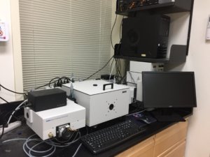
__________________________________________________________________
Spin and Spray Coating
Solution processing of metals, semiconductors and insulators is a way of cheaply and quickly building complex electronic devices that are thin, lightweight and flexible.
Atomic Force Microscopy (AFM)
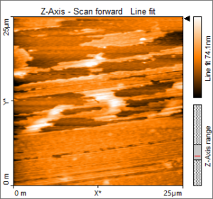
AFM is a tool used to image nanometer scale materials to obtain information about particle sizes, film thicknesses, film roughness and surface morphology on features that are 400 times smaller than is possible with the optical microscope. Single atomic monolayers have been imaged with this type of microscopy.
Air-free Schlenk Line Synthesis
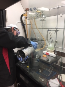
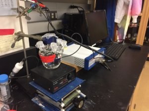
Schlenk-line glassware is used to conduct syntheses of nanomaterials or single molecules. We use this set-up for a variety of reactions.
3D Printing
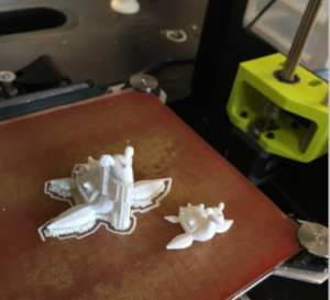
This rapidly growing area of materials science involves additive manufacturing, or building by adding onto the previous layer. We have several plastic 3D printers on campus; however, the Materials Science program has the capability to print with a range of extremely rigid plastics to extremely flexible. We also have an extruder for developing composite plastic filaments to build structures from scratch with your design that are fluorescent, conductive or perhaps contain a functional chemical.
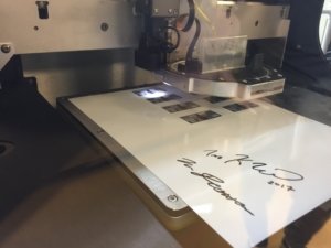
2D Electronic Printing
2D printing of electronics involves synthesis of nanocrystal ink or pre-cursor salt solution and printing layer by layer of metallic and semiconducting layers to build ultrathin lightweight and flexible devices all produced with the controlled automated printing process.
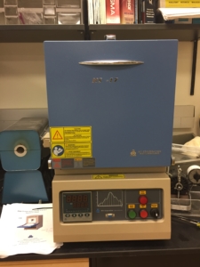
High Temperature Furnace
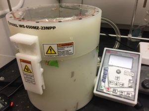
Furnaces like this can reach 1700C and are used to conduct solid state synthesis of inorganic materials. Typically, metal oxides are mixed in the desired stoichiometric ratios and heated to form new crystals with unique properties.
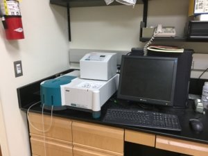
UV/Vis Spectrophotometry
UV-light and Visible light are scanned along the energy scale to illuminate your sample. Here we get a snap-shot of the wavelengths of light that your sample absorbs.
Electrochemistry
Electrochemistry is a versatile tool for understanding how easily films oxidize (rust, lose electrons) or reduce (gain electrons). By comparing your material to a standard electrode, we can learn what effects your experiments will have on the ability of your material to decompose, to produce oxygen, to produce hydrogen, or how light will impact this.
X-ray Fluorescence
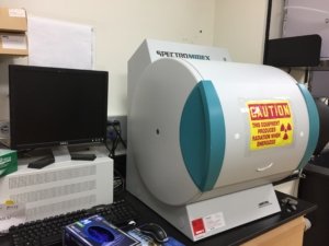
XRF is used to determine which elements are composing you material. X-rays are illuminated onto your sample, and elements will absorb this light and fluoresce at their elemental light signature. In this way, specific elements can be detected.
Hall Measurement System
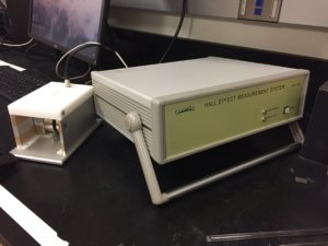
Based on the Hall Effect, a magnetic field is applied across your thin sample to disrupt the flow of electrons or holes (lack of electrons). From the voltage that is generated by the magnet, we can calculate the density of charge carriers (electrons or holes), the mobility of these carriers (how easily they move), and the conductivity of your material.
Solar Simulation Testing System
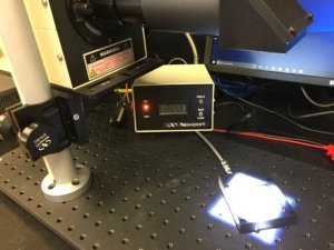
This machine delivers calibrated 1 sun illumination for calculating current-voltage plots for our research photovoltaic devices.
UV/Vis Flourescence
Fluorescence occurs after excitation of your material with light. The light energy is absorbed and then re-emitted (often at a lower energy). This machine characterizes both the wavelength(s) of light that are emitted, and also the intensity of that light.
Scanning Electron Microscopy (SEM)

Like AFM, SEM produces images of nanomaterials. We provide our students with SEM images of their materials through partnerships with the Naval Research Laboratory and Pax River NAVAIR
X-ray Diffraction
We have plans to write a grant for this instrument! It can tell you what type of crystal you have and its phase based on referencing to a database of XRD patterns.
Materials Science Academic Offerings
Why Study Materials Science?
Courses

